Tom Narwid
Well-Known Member
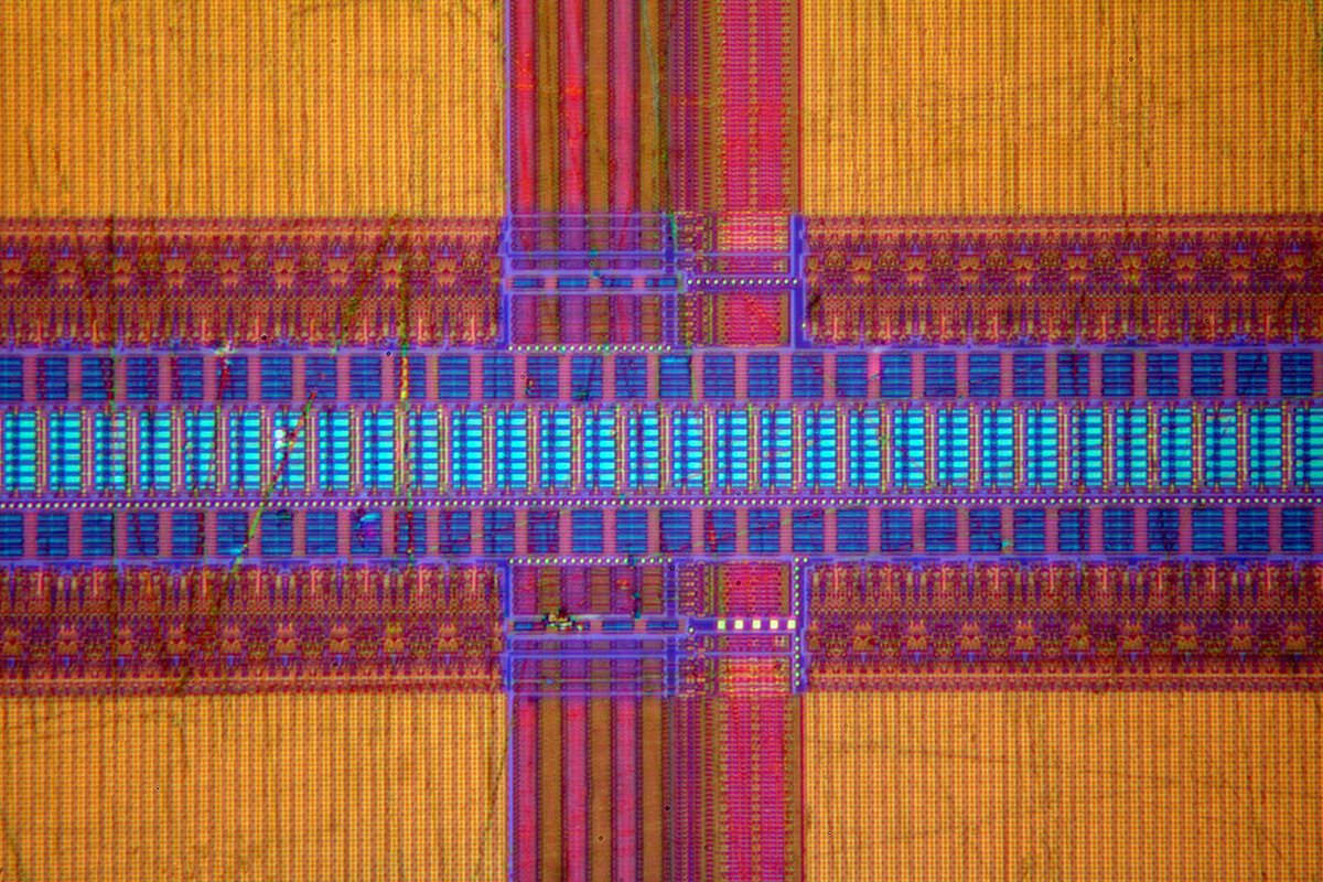
Vintage AMD Opteron Microprocessor (circa 2006)
")
I believe you are right Jameel. To get to any size detail one will need to spend $2000-4000 for an objective if they even make one. A scanning electron microscope!!!!Nice abstract and interesting to see the details. With todays 7nm (and soon even smaller) geometries, one will need crazy amount of magnification to see this level of detail.
Hey Ken. Thanks for your comment. If you have not seen the video I posted yet here is the YouTube url:I find this very interesting Tom. I worked for IBM as an engineer in the early 70's and at that time they were the largest manufacturer of integrated circuits in the world. I remember breaking one open to have a look. The degree of integration was slight with approx 10 elements per chip and the circuitry could be seen and understood with the naked eye. The technology was RTL a precursor of TTL which in its turn made way for CMOS which is still current today. Ken
500-600xHey Tom,
This is so cool, very interesting to see. How much is this magnified?